Objective:
The purpose of today's lesson is to understand operational amplifiers which is a unit that behaves like a voltage controlled voltage source. We can see that operational amplifiers only run on negative feedback by tying the output voltage to the the negative feedback. We focus on the 741 operational amplifier which has 8 pins of different terminals which can be seen in Figure 1. However, we will consider the OP 47 as seen in Figure 2 for the Lab called Inverting Voltage Amplifier. We also learn the process of replacing the operational amplifier with an equivalent circuit model. The process can be followed by seeing Figure 3.
 |
| Figure 1. Schematic for 741 operational amplifier. |
 |
| Figure 2. Schematic for OP27 operation amplifier. |
Group Practice:
1. Figure 4 shows a problem in which we are told to redraw the equivalent circuit of the operational amplifier based in Figure 3. We are told to find the loop gain Vo/Vs. We found the Vo/Vs = 9.0041 by using nodal voltage analysis as seen in Figure 4.
 |
| Figure 3. Process on how to replace an operational amplifier with an equivalent circuit. |
 |
| Figure 4. Class practice |
Lab Procedures and Results:
1. As part of the pre lab, we design an inverting amplifier where it provides a gain of 2 and R1 = 2K. The design can be seen in figure 5 and find the R2 = 4K by understanding that R2/R1 is the gain of the amplifier. However, we can not use theses exact resistance since it is not available instead we look at the E12 Values of resistors which can be seen in figure 6. We find that R1 = 2.2K and R2 = 4.7K which is the closest to the theoretical resistors.
 |
| Figure 5. Replacing the operational amplifier with an equivalent circuit. |
 |
| Figure 6. Table will help find the necessary E12 values needed for the circuit. |
2. We begin with the experiment by measuring the exact resistance of the resistors where
R1=2.14K=/-.01 and
R2 = 4.64K+/-.01 which can be seen in figure 7 and 8, respectively.
 |
| Figure 7. Measure resistance of R1 = 2.14K+/-.01 |
 |
| Figure 8. Measured resistance for R2 = 4.64K=/-.01 |
3. We then design the actual circuit as seen in figure 9 based on our design We generate a voltage input of -3V to 4V by intervals of .5V.
 |
| Figure 9. Actual inverting amplifier design circuit. |
4. We measure the output voltage when the input voltage was -3V and found that output voltage measured Vout=-3.41V+/-.01. We then increased the voltage by intervals of .5 up to 4V. The output voltage when the input voltage was 4V gave us a measurement of Vout=4.12V+/-.01. The experimental can be seeing figures 10 to 12.
 |
| Figure 10. Measured output voltage of -3.41V when the input voltage was 4V. |
 |
Figure 11. Measure output voltage of 4.21V when the input voltage was -3V
|
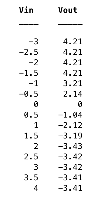
5. We then plot the measurements in a V out vs Vin plot. We can see that the output voltage is restricted by
4.21<Vo<-3.43. When the input voltage increases above the linear range, the operational amplifier becomes saturated above linear region.
 |
| Figure 12. Measure values of Voltage in and voltage our. |
 |
| Figure 13. V out vs V in plot for lab |
Summary of Lab and Learning Outcome:
Our design of an inverting voltage amplifier shows that the relationship between the V in and V out is Vout/Vin = -R2/R1 which holds true based on our plot where the Vout/Vin is the slope of the Vout vs Vin plot as seen in Figure 13. We see that our slope based on curve fitting is
-2.57. Applying the gain of the amplifier, we acquire
2.17 which is close to our slope with a percent difference of
18.4%. The difference is not to large considering that the linear region is not perfectly linear. The plot shows us that the output voltage is restricted by
4.21<Vout<-3.43 and anything above that becomes saturated which can be seen as voltage output line flattens.


No comments:
Post a Comment